

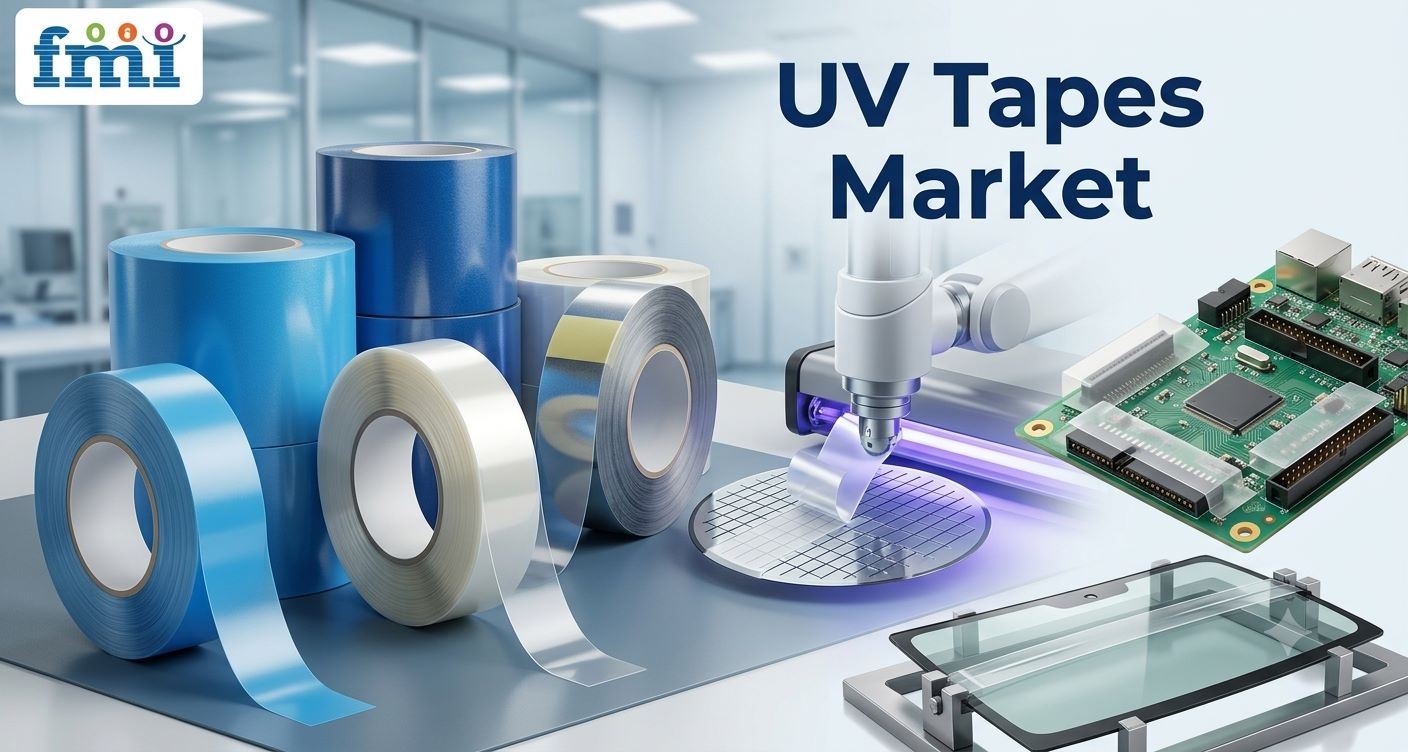
The UV tapes market is gaining traction as semiconductor manufacturers seek safer and more precise methods for wafer processing. UV tapes are used to protect semiconductor wafers during backgrinding, wafer dicing, and package dicing. As a result, their ability to protect wafers and support easy removal after UV irradiation is driving demand.
ok
The UV tapes market is expected to expand as semiconductor manufacturing becomes more focused on precision and miniaturization. UV tapes help secure semiconductor wafers during grinding and dicing while providing a controlled method for removal.
The semiconductor industry remains the primary application area for UV tapes. In addition, their use in wafer backgrinding and dicing supports demand as manufacturers seek improved processing efficiency.
Wafer Backgrinding Drives Application
Wafer backgrinding is one of the major applications for UV tapes. The process reduces semiconductor wafer thickness so that integrated circuits can be packaged efficiently.
Before backgrinding, manufacturers laminate wafers with UV tapes to protect them from grinding fluids. Therefore, the tape provides an additional layer of protection during a process that can expose wafers to mechanical stress and fluids.
After backgrinding, UV irradiation allows the tape to be removed from the wafer.
Wafer Dicing Supports Demand
UV tapes are also widely used during semiconductor wafer dicing. Dicing separates individual dies from a semiconductor wafer so that they can be used in electronic packages.
Modern dicing processes are increasingly automated to improve precision and accuracy. In addition, UV tapes can help minimise chipping during the separation of semiconductor dies.
The tapes also provide benefits such as low contamination from ionic substances and easier die pick-up.
UV Tapes Offer Processing Advantages
UV tapes provide several advantages over conventional PSA tapes. Their thin construction allows them to settle seamlessly onto semiconductor wafers during processing.
UV irradiation also changes the adhesion characteristics of the tape, making removal easier after wafer processing. As a result, manufacturers can remove the tape without creating excessive stress or leaving adhesive residues.
High Costs Limit Adoption
Despite their processing advantages, UV tapes still represent a small portion of the overall pressure sensitive adhesives market. According to Future Market Insights, UV tapes accounted for less than 1% of global PSA tape revenue share in 2014.
High costs remain one of the main barriers to adoption. Therefore, some semiconductor manufacturers may continue to use conventional alternatives where cost considerations outweigh the performance benefits of UV tapes.
Miniaturization Creates Growth Opportunities
The global consumer electronics industry is increasingly focused on smaller and lighter devices. As a result, semiconductor manufacturers are under pressure to produce compact and lightweight integrated circuits.
This trend can create opportunities for UV tapes because wafer processing becomes increasingly important as semiconductor components become smaller. In addition, the use of UV tapes in applications such as camera lens production demonstrates how changing consumer preferences can create new opportunities.
Growth Opportunities
The market offers opportunities as semiconductor manufacturing expands and electronics become smaller and more sophisticated. In addition, manufacturers can benefit from the use of UV tapes in applications that require precision and controlled adhesive removal.
Key opportunities include UV tape applications in:
- Wafer backgrinding
- Wafer dicing
- Package dicing
- Semiconductor manufacturing
- Camera lens production
- Compact consumer electronics
- Lightweight integrated circuits
Market Challenges
The UV tapes market faces several challenges, particularly related to cost and adoption. UV tapes currently account for a small share of the broader PSA tapes market. As a result, manufacturers need to demonstrate clear processing and performance benefits to justify their higher cost.
The semiconductor industry also requires highly controlled manufacturing processes. Therefore, UV tape manufacturers must maintain consistent adhesive performance, clean removal, and reliable wafer protection.
Regional Market Outlook
Asia Pacific remains an important region for the global UV tapes market. Demand is expected to remain robust as semiconductor manufacturing expands across countries such as China and Taiwan.
China’s semiconductor industry is benefiting from favourable government policies and continued industry development. As a result, growth in semiconductor manufacturing can support demand for UV tapes.
Taiwan is another important market because it is home to major semiconductor manufacturing facilities, including those operated by Taiwan Semiconductor Manufacturing Company Ltd. and UMC Powerchip.
Competitive Landscape and Future Outlook
Competition in the UV tapes market is shaped by adhesive performance, wafer protection, removal characteristics, contamination control, and cost. Manufacturers are focused on meeting the demanding requirements of semiconductor processing.
The expansion of semiconductor manufacturing and continued miniaturization of consumer electronics are expected to support market growth. Furthermore, increasing demand for compact devices can encourage manufacturers to adopt processing solutions that support thinner and lighter integrated circuits.
According to Future Market Insights, the global UV tapes market is projected to expand at a CAGR of over 9% through 2020 and reach US$ 437.9 million by 2020.
Conclusion
The UV tapes market is gaining importance in semiconductor manufacturing because of its role in wafer backgrinding, wafer dicing, and package dicing. Its ability to protect wafers and enable clean removal after UV irradiation supports its use in precision manufacturing.
High costs remain a key barrier to wider adoption. However, semiconductor miniaturization and the growing demand for compact consumer electronics are creating new opportunities.
Explore More Related Studies Published by FMI Research:
Mineral Processing Dispersants Market
E-Coat Pretreatment Chemicals Market
FMI Custom Research: Strategic Intelligence for Confident Decision-Making
In today’s rapidly evolving business environment, leadership teams need more than market data—they need clear, actionable intelligence tailored to their strategic objectives. FMI’s Custom Research solutions are designed around the specific business questions organizations need answered, enabling executives to evaluate growth opportunities, validate investments, assess competitive dynamics, and reduce uncertainty before making critical decisions. By combining deep industry expertise, primary research, and proprietary market intelligence, FMI delivers insights that help organizations move from assumptions to evidence-based strategies with greater speed and confidence.
Key Executive Benefits
- Decision-Ready Insights: Research tailored to your specific business challenges, growth plans, and investment priorities.
- Reduced Strategic Risk: Validate market opportunities, customer demand, and competitive positioning before committing resources.
- Market Entry Confidence: Assess opportunity size, regulatory barriers, channel dynamics, and competitive landscapes with precision.
- Competitive Advantage: Gain proprietary intelligence unavailable through syndicated reports or internal datasets.
- Faster Growth Decisions: Accelerate expansion, product development, portfolio optimization, and investment planning.
- Primary Market Validation: Access real-world customer, buyer, and stakeholder insights that support high-confidence decision-making.
- Global Industry Expertise: Powered by 100+ analysts, 20,000+ published reports, and 1.6 million+ hours of research experience.
- Proven Track Record: Over 7,000 market-entry engagements completed across six regions and 14 industry sectors with strong client retention.
Business Impact
FMI helps organizations transform market complexity into strategic clarity, enabling leadership teams to identify growth opportunities faster, optimize resource allocation, strengthen competitive positioning, and make high-stakes business decisions with confidence.
To explore how FMI Custom Research can support your strategic priorities, please connect with our team at – sales@futuremarketinsights.com
About Future Market Insights (FMI)
Future Market Insights is a leading provider of market intelligence, consulting services, and syndicated research reports. FMI delivers actionable insights across food and beverage, healthcare, consumer goods, biotechnology, chemicals, industrial products, and emerging technologies, helping organizations identify growth opportunities and make informed strategic decisions in evolving global markets.
Contact Us:
Future Market Insights Inc.
Christiana Corporate, 200 Continental Drive,
Suite 401, Newark, Delaware – 19713, USA
T: +1-347-918-3531
Why FMI: https://www.futuremarketinsights.com/why-fmi
For Sales Enquiries: sales@futuremarketinsights.com
Website: https://www.futuremarketinsights.com