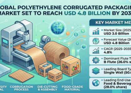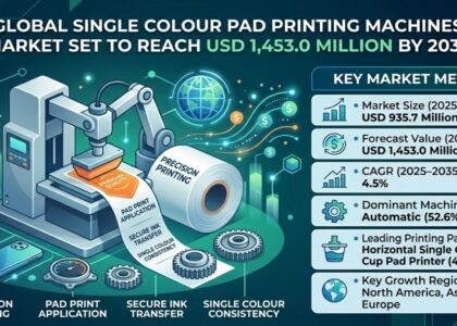
The semiconductor assembly and testing service industry is undergoing a structural transformation—and at the center of it is the United States. As traditional monolithic chip scaling runs into physical and economic limits, U.S. chipmakers are leading the global transition to chiplet-based processor architectures, supported by advanced 2.5D and 3D packaging technologies. Established giants like AMD, Intel, NVIDIA, Apple, and Qualcomm are setting the pace, while newer manufacturers and suppliers are rapidly aligning their strategies to participate in this high-growth ecosystem.
Why Chiplet Architectures Are Replacing Monolithic Designs
For decades, Moore’s Law guided performance gains through smaller transistors. But as dies approached reticle size limits and yields declined, economics began to break down. U.S. semiconductor companies were among the first to respond by disaggregating large chips into smaller, specialized chiplets.
AMD proved commercial viability in 2017 with its EPYC server processors. By separating compute dies built on advanced nodes from IO dies produced on mature, cost-efficient processes, AMD delivered 64-core processors at scale—something monolithic designs struggled to achieve. This approach dramatically improved yields and lowered cost per core, reshaping expectations across the server market.
Intel followed with its tile-based architecture, treating chiplets as modular building blocks. Compute tiles are fabricated on leading-edge nodes, while memory controllers and IO functions leverage mature processes. This strategy cuts total silicon cost by 30–40% and accelerates time-to-market by reusing validated tiles across multiple product families. For manufacturers looking to expand product portfolios efficiently, this model is becoming increasingly attractive.
NVIDIA extended chiplet adoption into GPUs with its Blackwell generation, splitting compute across dual dies linked by ultra-high-density interconnects exceeding 10 terabytes per second. Apple took a system-level approach with its M1 Ultra, bonding two full SoCs using UltraFusion technology to create a 114-billion-transistor processor that performs like a monolithic chip.
U.S. Leadership in 2.5D and 3D Packaging Innovation
Chiplets only work if packaging technologies can deliver massive bandwidth with minimal latency—and this is where U.S. innovation stands out.
Intel’s EMIB (Embedded Multi-die Interconnect Bridge) enables high-density connections without full silicon interposers, lowering cost while maintaining performance. Its Foveros technology goes further by enabling vertical die stacking using hybrid copper bonding with interconnect densities exceeding 10,000 connections per square millimeter. Combined in EMIB 3.5D architectures, these technologies support heterogeneous systems spanning multiple process nodes and more than 100 billion transistors in a single package.
AMD pioneered 3D V-Cache, stacking cache directly on compute dies using hybrid bonding. This approach delivers up to 96 MB of L3 cache per chiplet and bandwidth reaching 2 TB/s. In real-world workloads like computational fluid dynamics and electronic design automation, performance gains reach 50%, making this technology especially attractive to data center customers.
Apple leverages TSMC’s CoWoS packaging for its UltraFusion interconnect, achieving monolithic-like performance through 2.5D integration. This demonstrates how advanced packaging can deliver system-level gains without requiring single massive dies.
Why High Bandwidth Memory Integration Favors U.S.-Aligned Facilities
As AI and HPC workloads explode, High Bandwidth Memory (HBM) integration has become a critical differentiator—and one of the most complex manufacturing steps. HBM stacks require microbump pitches below 40 microns and placement accuracy within just 5 microns across large packages.
NVIDIA’s H100 GPU, for example, integrates five HBM3 stacks around a GPU die on a CoWoS interposer. Newer Blackwell GPUs push complexity further, demanding sub-micron alignment for die-to-die interconnect bridges. These challenges explain why advanced assembly, test, and validation—often accounting for 20–30% of total manufacturing cost—are concentrated in highly specialized, U.S.-aligned facilities.
Only a handful of locations worldwide have the equipment, automation, and process expertise to reliably test packages containing dozens of active dies operating at multi-terabyte-per-second bandwidths.
Supply Chain Strategy: Interposers, Substrates, and U.S. Alternatives
Silicon interposers remain a bottleneck, with TSMC dominating CoWoS production. As demand from AI accelerator vendors grows, packaging capacity constraints are becoming more visible. Intel’s EMIB approach offers a compelling alternative by avoiding full interposers and relying on advanced organic substrates instead.
Intel’s Rio Rancho, New Mexico facility now serves as a hub for EMIB and Foveros packaging, attracting interest from companies seeking diversification away from Asia-centric supply chains. However, substrate manufacturing remains a challenge. High-performance ABF substrates require fine-line capabilities approaching 2-micron dimensions, limiting qualified suppliers and creating opportunities for new entrants willing to invest in process innovation.
How U.S. Assembly and Test Capabilities Are Shaping the Future
The expansion of U.S.-based assembly and test is accelerating. Amkor Technology’s $2 billion advanced packaging facility in Arizona, scheduled for production by 2028, will support chiplets fabricated at nearby fabs. Apple’s early commitment signals strong confidence in domestic advanced packaging.
Meanwhile, Intel continues expanding EMIB and Foveros capacity across New Mexico, Arizona, and Oregon, positioning Intel Foundry Services as a full-stack manufacturing partner—from design to packaging and test.
The geographic clustering of fabs, packaging lines, and equipment suppliers in Arizona mirrors the ecosystem advantages once unique to Taiwan. For both established leaders and emerging manufacturers, this environment enables faster iteration, supply chain resilience, and scalable adoption of chiplet-based architectures—cementing U.S. leadership in the next era of semiconductor innovation.
A Full Report on Market: https://www.futuremarketinsights.com/articles/why-does-the-united-states-lead-in-chiplet-architecture-and-heterogeneous-integration