The Extreme Ultraviolet Lithography (EUV) market is projected to reach USD 12.3 billion in 2025 and expand to USD 28.5 billion by 2035, registering a CAGR of 9.2% over the forecast period. The growth is driven by increased investments from semiconductor manufacturers and ongoing R&D to improve EUV throughput and efficiency in chip fabrication.
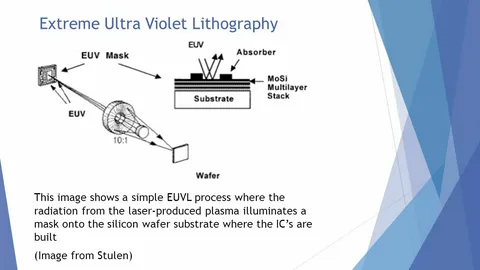
The extreme ultraviolet lithography market is gaining significant traction as the semiconductor industry continues its push toward smaller, more powerful, and more efficient devices. Extreme ultraviolet (EUV) lithography is a next-generation technology used in semiconductor manufacturing, particularly for producing integrated circuits at smaller nodes. This advanced technique utilizes light with extremely short wavelengths to enable higher resolution patterning than traditional lithography methods. As consumer electronics demand more compact and energy-efficient chips, EUV lithography is becoming indispensable for chipmakers worldwide.
The extreme ultraviolet lithography market is being driven by the need for technological advancement and the growing requirement for miniaturization in electronic devices. Traditional photolithography methods are becoming less effective at smaller scales, making EUV lithography a viable alternative for continued innovation. As the industry moves toward 5nm and even 3nm process nodes, EUV technology will become increasingly critical in ensuring production efficiency, accuracy, and scalability.
Get Sample Report: – https://www.futuremarketinsights.com/reports/sample/rep-gb-5871
Size & Trends
The extreme ultraviolet lithography market is witnessing consistent growth, fueled by increased demand for advanced semiconductors in applications ranging from smartphones and laptops to automotive and industrial electronics. The expansion of data centers, artificial intelligence, and 5G infrastructure also contributes to the rising adoption of EUV technology. With ongoing investments by key semiconductor foundries and original equipment manufacturers, the market is expected to maintain a positive growth trajectory over the coming years.
Another notable trend shaping the extreme ultraviolet lithography market is the integration of EUV in high-volume manufacturing. As production yields improve and equipment becomes more accessible, major chipmakers are transitioning to EUV processes to stay competitive. The development of EUV-compatible photoresists and mask technologies further enhances the viability of this cutting-edge solution. Additionally, strategic collaborations between technology providers and foundries are driving the acceleration of EUV adoption, ultimately reshaping the semiconductor manufacturing landscape.
Key Highlights
One of the most critical highlights of the extreme ultraviolet lithography market is its transformative impact on semiconductor design and fabrication. EUV lithography allows for smaller feature sizes, leading to higher transistor densities and improved performance-per-watt ratios. This directly translates into faster, more efficient electronic devices, which are in high demand across consumer, industrial, and enterprise sectors.
Another important aspect is the substantial investment being funneled into EUV R&D and infrastructure. Leading players are committing resources to refine the technology, increase throughput, and reduce costs associated with EUV equipment. Moreover, national governments and research institutions are also supporting EUV initiatives, recognizing the strategic importance of semiconductor independence. These investments are helping to build a more robust and sustainable EUV ecosystem, further enhancing the market’s long-term prospects.
Challenges and Opportunities
Despite its promise, the extreme ultraviolet lithography market faces several challenges that could slow its adoption. One major hurdle is the high cost of EUV equipment, which can be a barrier for smaller semiconductor companies. The complexity of integrating EUV into existing production lines also poses significant technical challenges, requiring extensive training, cleanroom modifications, and system recalibrations.
However, these challenges are accompanied by numerous opportunities. As EUV technology matures and scales, economies of scale are expected to bring down costs, making it accessible to a broader range of manufacturers. Furthermore, ongoing innovation in supporting technologies, such as pellicles and defect-inspection systems, will address current technical limitations and enhance overall productivity. The increasing focus on domestic semiconductor production across various regions also presents a growth opportunity for EUV suppliers, as countries seek to secure their chip supply chains through advanced manufacturing capabilities.
Key Benefits for Stakeholders
Stakeholders across the extreme ultraviolet lithography market stand to gain significantly from the continued development and deployment of EUV technology. Semiconductor manufacturers benefit from enhanced precision and scalability, enabling them to produce smaller and more powerful chips. This leads to improved competitiveness and the ability to meet the growing demands of advanced computing applications.
For equipment vendors, EUV represents a high-value product segment with long-term growth potential. As adoption rises, these companies can capitalize on service contracts, upgrades, and maintenance opportunities. Additionally, end-users, including OEMs in consumer electronics and automotive sectors, benefit from better-performing devices that consume less power and occupy less space, thereby enhancing user experience and reducing environmental impact.
Government and academic stakeholders also reap benefits from a strong EUV infrastructure. It fosters innovation, supports domestic technology leadership, and creates high-skilled job opportunities in engineering and manufacturing. Altogether, the broad array of advantages makes the extreme ultraviolet lithography market a highly strategic domain for stakeholders across the value chain.
Market Share by Geographical Region
The extreme ultraviolet lithography market is geographically concentrated, with significant contributions from regions with advanced semiconductor manufacturing capabilities. Asia-Pacific holds a dominant position, driven by countries like Taiwan, South Korea, and China. These nations are home to some of the world’s largest chipmakers, who are actively incorporating EUV into their manufacturing processes.
North America is another major player in the extreme ultraviolet lithography market, particularly due to the presence of leading technology providers and research institutions. The U.S. government’s focus on semiconductor self-reliance is further fueling investments in EUV technologies, making the region a key driver of innovation and commercialization.
Europe also plays a critical role, especially as it is home to some of the most prominent EUV equipment manufacturers. Strong research collaboration and public-private partnerships are accelerating the region’s EUV capabilities. As countries globally invest in semiconductor independence and resilience, the geographical distribution of EUV market share is expected to diversify further over the next decade.
Competitive Outlook
The competitive landscape of the extreme ultraviolet lithography market is shaped by a few dominant players with specialized capabilities in high-precision optical systems and advanced semiconductor manufacturing equipment. These companies are constantly engaged in research and development to enhance system reliability, reduce downtime, and increase wafer throughput.
The market is also witnessing growing collaboration among stakeholders to develop end-to-end EUV solutions. Equipment vendors are working closely with semiconductor foundries to fine-tune processes, while material suppliers are developing photoresists and masks that can withstand the rigors of EUV exposure. This integrated approach is essential for overcoming technical challenges and realizing the full potential of the technology.
In addition to technological innovation, strategic partnerships and mergers are becoming increasingly common as companies look to consolidate capabilities and expand their market reach. Intellectual property, service quality, and customer relationships are key differentiators that determine success in this competitive environment.
Top Companies
Several key players dominate the extreme ultraviolet lithography market, each contributing uniquely to the technology’s development and deployment. Among the most influential is a Dutch company widely recognized for its EUV lithography systems. Their machines are at the core of high-volume EUV production worldwide, making them a cornerstone of the market.
Other important contributors include major semiconductor foundries in Asia, which are early adopters of EUV in commercial chip manufacturing. These companies not only utilize EUV tools but also actively invest in their evolution through joint development agreements and infrastructure expansions.
Material suppliers and optics manufacturers also play critical roles. They provide essential components such as EUV photoresists, pellicles, and mirrors that withstand high-energy exposure. Their innovation is vital to overcoming current EUV limitations and achieving greater efficiency. Collectively, these top companies form a robust and collaborative ecosystem that continues to drive the extreme ultraviolet lithography market forward.
Explore In-Depth Analysis-Click Here to Access the Report:- https://www.futuremarketinsights.com/reports/extreme-ultraviolet-lithography-market
Segmentation Outlook
- The extreme ultraviolet lithography market can be segmented based on equipment type, end-user industry, and application. In terms of equipment, key segments include light sources, mirrors, photoresists, and mask infrastructure. Each of these components is critical to the success of EUV systems and requires high precision and durability.
- By end-user industry, the market is dominated by semiconductor foundries, integrated device manufacturers, and research institutions. Foundries are the largest consumers due to their role in mass chip production. Meanwhile, IDMs benefit from in-house integration of EUV tools for proprietary chip designs. Research institutions also play a supporting role in developing and testing next-generation EUV technologies.
- Application-wise, the primary focus is on logic and memory chips used in a variety of devices, from smartphones to servers. As demand grows for high-performance computing, edge devices, and AI applications, the need for advanced lithography solutions becomes even more pressing. Each segment contributes to the overall vibrancy and dynamism of the extreme ultraviolet lithography market.
About Future Market Insights (FMI)
Future Market Insights, Inc. (ESOMAR certified, recipient of the Stevie Award, and a member of the Greater New York Chamber of Commerce) offers profound insights into the driving factors that are boosting demand in the market. FMI stands as the leading global provider of market intelligence, advisory services, consulting, and events for the Packaging, Food and Beverage, Consumer Technology, Healthcare, Industrial, and Chemicals markets. With a vast team of over 400 analysts worldwide, FMI provides global, regional, and local expertise on diverse domains and industry trends across more than 110 countries.
Contact Us:
Future Market Insights Inc.
Christiana Corporate, 200 Continental Drive,
Suite 401, Newark, Delaware – 19713, USA
T: +1-347-918-3531
For Sales Enquiries: sales@futuremarketinsights.com
Website: https://www.futuremarketinsights.com
LinkedIn| Twitter| Blogs | YouTube

