
Market Overview: Advanced Semiconductor Packaging Gains Momentum with AI and Miniaturization Trends
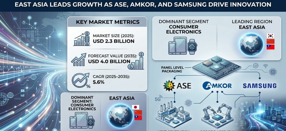
The global panel level packaging (PLP) market is witnessing strong expansion, driven by the rapid evolution of semiconductor technologies and the growing demand for compact, high-performance electronic devices. The market is projected to grow from USD 2.3 billion in 2025 to USD 4.0 billion by 2035, registering a CAGR of 5.6% during the forecast period.
Panel-level packaging has emerged as a transformative solution in semiconductor manufacturing, offering higher throughput, improved cost efficiency, and enhanced design flexibility compared to traditional wafer-level packaging. As industries push toward miniaturization and higher input/output (I/O) density, PLP is becoming a preferred choice for next-generation chip production.
The rise of artificial intelligence (AI), high-performance computing (HPC), 5G, and Internet of Things (IoT) devices is accelerating the need for advanced packaging technologies. Panel-level packaging addresses these demands by enabling scalable, energy-efficient, and high-yield production processes.
Key Market Metrics
- Market Size (2025): USD 2.3 Billion
- Forecast Value (2035): USD 4.0 Billion
- CAGR (2025–2035): 5.6%
- Dominant Segment: Consumer Electronics
- Leading Region: East Asia
Get detailed market forecasts, competitive benchmarking, and pricing trends:
https://www.futuremarketinsights.com/reports/sample/rep-gb-16680
Key Demand Drivers
- Rising Demand for Miniaturized Electronics
The proliferation of smartphones, wearables, and compact computing devices has significantly increased the need for smaller yet more powerful semiconductor components. Panel-level packaging enables higher integration density while maintaining performance and efficiency.
- Growth of AI, 5G, and IoT Applications
Emerging technologies such as AI chips, 5G infrastructure, and IoT ecosystems require advanced packaging solutions capable of handling complex architectures. PLP supports these requirements with improved electrical performance and thermal management.
- Cost-Effective and Scalable Manufacturing
Compared to traditional packaging methods, PLP offers larger panel sizes, enabling mass production and reducing cost per unit. This scalability makes it ideal for high-volume consumer electronics manufacturing.
- Sustainability and Eco-Friendly Materials
With increasing regulatory pressure, manufacturers are shifting toward low-emission, lead-free, and recyclable materials. PLP contributes to sustainability by reducing material waste and improving energy efficiency during production.
Supply Chain Analysis: Who Supplies Whom
The panel level packaging ecosystem operates through a highly integrated value chain:
- Material Suppliers: Provide substrates such as silicon, glass, and organic materials along with interconnect materials.
- Equipment Providers: Deliver lithography, alignment, and automation tools for precision manufacturing.
- OSAT Companies: Firms like ASE Group and Amkor Technology handle outsourced semiconductor assembly and testing.
- Foundries & Chipmakers: Companies such as Samsung Electronics and TSMC integrate PLP into advanced chip fabrication.
- End-Use Industries: Consumer electronics, automotive, telecom, and healthcare sectors utilize packaged semiconductors.
Pricing Trends & Cost Dynamics
- Material Costs: High-quality substrates and advanced materials increase initial production costs.
- Economies of Scale: Larger panel sizes reduce per-unit cost, improving profitability.
- Automation Benefits: AI-driven manufacturing lowers scrap rates and enhances yield.
- Customization Premium: Advanced packaging for AI and HPC applications commands higher margins.
Segmentation Insights
By Technology Type
- Fan-out Panel-Level Packaging (FO-PLP)
- Wafer-Level Packaging (WLP)
- Panel-Level System-in-Package
- Embedded Die Panel Packaging
By Carrier Type
- Rigid Carrier (dominant due to stability and precision)
- Flexible Carrier
- Organic Substrate Carrier
- Glass, Metal, and Composite Carriers
By End Use
- Consumer Electronics (largest segment)
- Automotive Electronics
- Telecommunications
- Aerospace & Defense
- Healthcare Devices
Regional Analysis
East Asia: The Global Powerhouse
East Asia dominates the PLP market, driven by strong semiconductor ecosystems in China, South Korea, and Japan. High investments in AI chips, 5G infrastructure, and domestic chip manufacturing are fueling growth.
North America: Innovation Hub
The region benefits from advanced R&D, strong presence of chipmakers, and growing demand for AI and autonomous technologies. Increasing investments in domestic semiconductor manufacturing further support market expansion.
Europe: Sustainability-Driven Growth
Europe is focusing on eco-friendly semiconductor production and strengthening supply chains through initiatives like the European Chips Act. Automotive and industrial electronics demand is a key growth driver.
Unlock 360° insights for strategic decision making and investment planning: https://www.futuremarketinsights.com/checkout/16680
Competitive Landscape
The panel-level packaging market is moderately consolidated, with leading players focusing on innovation, automation, and sustainability.
Key Players and Market Presence
- ASE Group
- Amkor Technology
- Samsung Electronics
- Qualcomm
- Broadcom Inc.
- NXP Semiconductors
- STMicroelectronics
- Kyocera Corporation
Strategic Focus Areas
- Development of advanced fan-out and 3D packaging technologies
- Investment in eco-friendly and low-emission materials
- Expansion of AI and HPC packaging capabilities
- Strategic partnerships and acquisitions
- Automation and smart manufacturing integration
Technology & Innovation Trends
- AI-Powered Manufacturing: Enhances defect detection and yield optimization
- Hybrid Bonding & 3D Stacking: Enables higher integration density
- Fan-Out Architectures: Improve electrical performance and reduce footprint
- Large Panel Substrates: Support mass production and cost efficiency
- Eco-Friendly Materials: Reduce environmental impact and meet regulatory standards
Challenges
- High capital investment requirements
- Complexity in integrating PLP with existing semiconductor processes
- Volatility in raw material costs
- Technical barriers in large-scale adoption
Opportunities & Investment Outlook
- AI & Edge Computing: Growing demand for advanced chip packaging
- Automotive Electronics: Expansion of EVs and autonomous systems
- Emerging Markets: India and Southeast Asia offer strong growth potential
- Sustainability Initiatives: Development of recyclable and biodegradable materials
- Strategic Collaborations: Partnerships between foundries and OSAT providers
Speak to Analyst: Customize insights for your business strategy: https://www.futuremarketinsights.com/customization-available/rep-gb-16680
Future Outlook (2025–2035)
The panel-level packaging market is expected to evolve into a cornerstone of next-generation semiconductor manufacturing. As device complexity increases and demand for performance intensifies, PLP will play a critical role in enabling scalable, efficient, and sustainable production.
Future growth will be driven by advancements in AI hardware, 5G networks, and IoT ecosystems. Additionally, increasing focus on circular manufacturing and eco-efficient processes will reshape industry standards.
By 2035, companies that prioritize innovation, sustainability, and high-volume manufacturing capabilities will gain a competitive edge. Panel-level packaging will transition from a niche technology to a mainstream solution, supporting the global demand for faster, smaller, and more efficient electronic devices.
Why FMI: https://www.futuremarketinsights.com/why-fmi
About Future Market Insights (FMI)
Future Market Insights, Inc. (FMI) is an ESOMAR-certified, ISO 9001:2015 market research and consulting organization, trusted by Fortune 500 clients and global enterprises. With operations in the U.S., UK, India, and Dubai, FMI provides data-backed insights and strategic intelligence across 30+ industries and 1200 markets worldwide.
Contact Us:
Future Market Insights Inc., Christiana Corporate, 200 Continental Drive, Suite 401, Newark, Delaware – 19713, USA
T: +1-347-918-3531
For Sales Enquiries: sales@futuremarketinsights.com
Website: https://www.futuremarketinsights.com
LinkedIn| Twitter| Blogs | YouTube