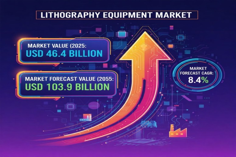
The global lithography equipment market is on a remarkable growth trajectory, projected to rise from USD 46.4 billion in 2025 to USD 103.9 billion by 2035, reflecting a robust compound annual growth rate (CAGR) of 8.4%. This surge highlights the critical role of lithography systems in semiconductor manufacturing, advanced packaging, and next-generation electronics, where precision, miniaturization, and high-throughput production are increasingly essential.
During the early adoption phase between 2020 and 2024, the market expanded gradually from USD 31.0 billion to USD 46.4 billion. This period was marked by pilot deployments and validation of next-generation lithography systems, as semiconductor manufacturers sought higher precision and smaller node production. Operational efficiency improvements and performance validation for next-generation chips laid the foundation for broader adoption starting in 2025.
Scaling and Consolidation: Market Evolution Through 2035
From 2025 onward, the lithography equipment market enters a scaling phase, projected to surpass USD 64.1 billion by 2030, driven by high-volume semiconductor manufacturing and expansion of production capacities. The subsequent consolidation phase, stretching to 2035, anticipates continued growth toward USD 103.9 billion as leading suppliers dominate the landscape while smaller players align with established ecosystems or exit the market.
This steady 8.4% CAGR reflects a transition from experimental adoption to broad integration, positioning lithography equipment as a core component of mainstream semiconductor production worldwide.
Technological and Equipment Highlights
Extreme Ultraviolet (EUV) lithography emerges as the leading technology segment, expected to account for 42.6% of market revenue in 2025. EUV systems enable sub-10 nanometer patterning, essential for advanced logic chips, high-density memory, and next-generation processors.
Their scalability, precision, and capability to handle complex multi-layer architectures with reduced defect rates make EUV systems a preferred choice for semiconductor manufacturers pursuing Moore’s law. Investments in supporting infrastructure, such as advanced optics and enhanced source power, are further accelerating EUV adoption.
In terms of equipment type, Optical Lithography/Photolithography dominates with a 47.9% revenue share in 2025. Its reliability, cost-effectiveness, and adaptability across wafer sizes and device types make it indispensable, particularly for mature technology nodes. Continuous improvements in immersion lithography, stepper, and scanner technologies have enhanced performance and resolution, allowing optical lithography to remain a cornerstone of high-volume semiconductor fabrication.
Advanced Packaging Drives Application Growth
The Advanced Packaging segment represents the largest application area, contributing 38.4% of market revenue in 2025. The rise of wafer-level packaging, system-in-package, and 3D stacking technologies has increased the demand for high-precision lithography systems capable of patterning fine features.
High-performance computing, AI, automotive electronics, and 5G communications are primary drivers of advanced packaging adoption. By enabling smaller interconnect pitches and improved electrical performance, lithography equipment plays a crucial role in delivering miniaturized, energy-efficient, and high-performance devices.
Global Growth Drivers and Market Dynamics
The lithography equipment market growth is fueled by increasing semiconductor demand, ongoing miniaturization of integrated circuits, and adoption of advanced fabrication technologies. North America and Europe lead in high-precision EUV and deep ultraviolet (DUV) lithography for cutting-edge chip manufacturing, while Asia-Pacific experiences rapid growth driven by expanding foundries and electronics production.
Resolution and wafer throughput capabilities significantly influence adoption. North American and European markets emphasize sub-5nm node fabrication for AI and high-performance computing chips, requiring precise alignment, defect-free exposure, and rapid processing speed. Meanwhile, Asia-Pacific balances performance and cost, deploying DUV and mid-range lithography tools for mass-market electronics and consumer devices.
Reliability, uptime, and maintenance also impact market adoption. High-reliability systems with predictive maintenance and remote diagnostics dominate in mature regions, while modular, serviceable designs cater to high-volume, cost-sensitive markets in emerging regions. Integration with the broader semiconductor ecosystem, including photomasks, metrology tools, and automation systems, further shapes market value and adoption rates.
Regional Market Insights
China leads growth among BRICS nations, with a CAGR of 11.3%, driven by large-scale semiconductor production, high-tech manufacturing initiatives, and strong government support. Investments in high-precision, automated, and energy-efficient lithography systems are accelerating adoption, positioning China as a global leader in lithography equipment.
India follows closely with a 10.5% CAGR, supported by expanding semiconductor and electronics manufacturing infrastructure. Government programs promoting domestic electronics, semiconductor self-reliance, and research infrastructure facilitate the adoption of advanced photolithography systems.
In Europe, Germany exhibits a 9.7% CAGR, underpinned by strong semiconductor, electronics, and automotive industries. Advanced resolution, automation, and energy efficiency are central to adoption. The United Kingdom, growing at 8.0% CAGR, benefits from government support for semiconductor research and high-tech manufacturing.
The United States, with a 7.1% CAGR, remains a mature market characterized by technological readiness and strong adoption of automated, high-precision lithography systems. Investments in semiconductor technology and electronics R&D further support equipment deployment across industrial and research applications.
Competitive Landscape: Leading and Emerging Players
The lithography equipment market is highly competitive, with established leaders and emerging players innovating to expand their footprint. ASML Holding N.V. dominates with EUV systems, enabling smaller, more efficient, and high-performing devices. Nikon Corporation and Canon Inc. continue to innovate in immersion lithography and stepper technologies for high-volume fabs.
Veeco Instruments Inc., SUSS MicroTec AG, and EV Group specialize in wafer bonding, nanoimprint, and photolithography solutions, supporting advanced packaging and MEMS production. SCREEN Holdings Co., Ltd., Onto Innovation Inc., JEOL Ltd., and Neutronix Quintel Inc. (NXQ) focus on inspection, metrology, and electron-beam lithography, ensuring precision and process reliability. Advantest provides integrated lithography test and inspection solutions, while Shanghai Micro Electronics Equipment (Group) Co., Ltd. delivers scalable, cost-effective systems tailored for emerging semiconductor markets in Asia.
Get this Report at $5,000 Only | Exclusive Discount Inside!
https://www.futuremarketinsights.com/reports/sample/rep-gb-25461
Checkout Now to Access Industry Insights:
https://www.futuremarketinsights.com/checkout/25461
About Future Market Insights (FMI)
Future Market Insights, Inc. (ESOMAR certified, recipient of the Stevie Award, and a member of the Greater New York Chamber of Commerce) offers profound insights into the driving factors that are boosting demand in the market. FMI stands as the leading global provider of market intelligence, advisory services, consulting, and events for the Packaging, Food and Beverage, Consumer Technology, Healthcare, Industrial, and Chemicals markets. With a vast team of over 400 analysts worldwide, FMI provides global, regional, and local expertise on diverse domains and industry trends across more than 110 countries.
Contact Us:
Future Market Insights Inc.
Christiana Corporate, 200 Continental Drive,
Suite 401, Newark, Delaware – 19713, USA
T: +1-347-918-3531
For Sales Enquiries: sales@futuremarketinsights.com
Website: https://www.futuremarketinsights.com
LinkedIn| Twitter| Blogs | YouTube