
The global semiconductor wafer market is poised for significant expansion, with projections indicating a rise from USD 24,362.2 million in 2025 to USD 42,987.0 million by 2035, reflecting a robust Compound Annual Growth Rate (CAGR) of 4.7%. This growth underscores the critical role of semiconductor wafers as the foundational material for integrated circuits and microdevices, essential components driving the modern electronics industry.
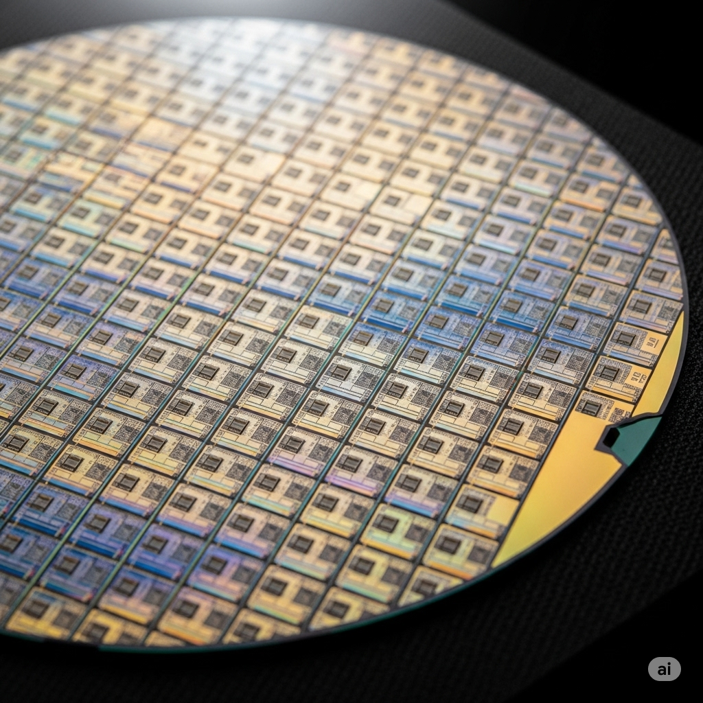
Semiconductor wafers, typically thin slices of silicon, are the raw materials from which chipsets are fabricated through intricate doping, etching, and deposition processes. Their high purity, consistency, and ability to enable miniaturization are pivotal for enhancing electronic component performance and packing more functionalities into smaller areas. The inherent advantage of fabricating multiple devices on a single substrate also boosts manufacturing capacity and reduces costs, aligning with industry trends towards efficiency.
Track Evolving Market Trends: Request Your Sample Report! https://www.futuremarketinsights.com/reports/sample/rep-gb-12824
Key Growth Drivers and Market Dynamics
The market’s upward trajectory is significantly propelled by the pervasive application of semiconductors across diverse industries, including automotive, consumer electronics, and telecommunications. From smartphones and laptops to advanced driver-assistance systems (ADAS) and infotainment in vehicles, wafers are indispensable. Governments worldwide are also actively supporting the semiconductor industry through strategic investments, recognizing its importance for digitization efforts. A notable example is Canada’s USD 90 million funding in July 2024 for the Fabrication of Integrated Components for the Internet’s Edge (FABrIC) network, managed by CMC Microsystems, aimed at fostering innovation and talent development. Similarly, international collaborations, such as the May 2024 pact between Brazil and Malaysia, further strengthen the global semiconductor ecosystem.
A major industry trend driving growth is the transition towards larger semiconductor wafers, particularly 300 mm and above. These larger wafers offer superior cost-effectiveness and efficiency compared to their 200 mm counterparts, enabling manufacturers to produce more chips per wafer and reduce per-unit manufacturing costs. This scalability is crucial for meeting the escalating demand for semiconductors in emerging technologies like 5G and the Internet of Things (IoT). In a significant move, the U.S. Commerce Department announced a USD 400 million grant to Global Wafers Co. Ltd. in July 2024 to establish the first 300-mm wafer foundry in the USA, aiming to bolster domestic supply chains and create approximately 880 manufacturing jobs.
The surge in automotive electronics, fueled by advancements in electric vehicles (EVs) and autonomous driving technologies, is another powerful catalyst. Semiconductor devices are integral to EV drivetrains, battery systems, and power management, as well as the high-performance computing required for ADAS and autonomous vehicles. The adoption of advanced functionalities like vehicle-to-everything (V2X) communication further amplifies demand. In August 2024, ASM committed USD 1.76 billion to a Japanese semiconductor manufacturing plant, focusing on hardware for industrial and automotive markets, underscoring this trend. Furthermore, rapid developments in 5G technologies are creating substantial opportunities, necessitating specialized semiconductor wafers capable of higher frequencies and faster data processing. Companies like SK Siltron Neveon are developing silicon carbide (SiC) and gallium nitride (GaN) wafers specifically for advanced 5G devices.
Challenges and Future Outlook
Despite robust growth, the market faces challenges related to technological complexity and environmental concerns. The relentless pursuit of smaller, faster, and cheaper chips demands increasingly intricate fabrication processes, including lithography, etching, and deposition, especially for advanced nodes like 5nm and below. This requires significant investment in sophisticated equipment and expertise to maintain high yields. Environmentally, wafer manufacturing is energy-intensive and involves toxic chemicals, prompting regulatory scrutiny and pushing manufacturers towards greener practices, which can increase production costs.
Looking ahead, the market is set to experience transformative shifts. From 2025 to 2035, governments are expected to heavily invest in domestic manufacturing to reduce import dependency. Technological advancements will see the adoption of 2nm and below process nodes, revolutionizing efficiency. AI-driven predictive analytics will optimize supply chains, and material innovations like quantum materials and 3D stacking will enhance performance. The proliferation of edge computing and quantum computing will further expand wafer demand.
Competitive Landscape and Regional Insights
The semiconductor wafer market is intensely competitive, driven by continuous innovation, wafer size, process node advancements, and factory efficiency. Tier 1 players, including Shin-Etsu Chemical Co., Ltd., SUMCO CORPORATION, Globalwafers Co. Ltd, Siltronic, and SK Siltron, command over 30% of the market. These leaders extensively invest in R&D to maintain their technological edge and global reach. Tier 2 companies, such as Okmetic, Wafer Works Corporation, LONGi Green Energy Technology Co., Ltd., and SOITEC, possess strong local market understanding and collaborate with technology service providers to innovate. Tier 3 players, comprising startups and SMEs, focus on niche, cost-effective solutions and rapid adaptation to market trends.
Regionally, the market exhibits dynamic growth. India is projected to lead with an impressive CAGR of 7.6% from 2025 to 2035, driven by substantial government investments, including USD 15 billion for three new semiconductor factories. China is expected to grow at a CAGR of 4.6%, propelled by rapid industrialization, technological advancements, and a high volume of semiconductor patent filings (55% in 2022). The USA, with a projected CAGR of 4.3%, continues to dominate the North American market, holding an estimated 78.9% share, fueled by increasing consumer demand for smart appliances and strategic domestic manufacturing initiatives.
In terms of application, consumer electronics are anticipated to witness substantial growth, with a projected CAGR of 14.2% from 2025 to 2035, driven by the increasing uptake of smartphones, laptops, tablets, and smart home devices. Within process nodes, 3nm technology is set to maintain its dominant share, capturing 15.6% in 2024. Its high efficiency, power, and transistor density make it critical for high-end consumer electronics, AI, and data centers, with major players like TSMC and Samsung continuing to prioritize its production.
The global semiconductor wafer market is at a pivotal juncture, characterized by robust growth, technological innovation, and strategic investments, all contributing to its indispensable role in the digital future.
Key players in the Semiconductor Wafer Industry
- Shin-Etsu Chemical Co., Ltd.
- SUMCO CORPORATION
- Globalwafers Co. Ltd
- Siltronic
- SK Siltron
- Okmetic
- Wafer Works Corporation
- LONGi Green Energy Technology Co., Ltd.
- Samsung
- SOITEC
Semiconductor Wafer Market Segmentation
By Process Node:
In terms of process node, the segment is divided into 3nm, 5nm, 7nm, 8nm, 10nm, 16nm, 20nm, 28nm, 40nm, and other nodes.
By Application:
The industry is classified by segment as automotive, consumer electronics, industrial manufacturing, telecommunications, and other applications.
By Region:
A regional analysis has been carried out in key countries of North America, Latin America, East Asia, South Asia & Pacific, Western Europe, Eastern Europe and Middle East and Africa (MEA), and Europe.
Buy Now: https://www.futuremarketinsights.com/checkout/12824
About Future Market Insights (FMI)
Future Market Insights, Inc. (ESOMAR certified, recipient of the Stevie Award, and a member of the Greater New York Chamber of Commerce) offers profound insights into the driving factors that are boosting demand in the market. FMI stands as the leading global provider of market intelligence, advisory services, consulting, and events for the Packaging, Food and Beverage, Consumer Technology, Healthcare, Industrial, and Chemicals markets. With a vast team of over 400 analysts worldwide, FMI provides global, regional, and local expertise on diverse domains and industry trends across more than 110 countries. Join us as we commemorate 10 years of delivering trusted market insights. Reflecting on a decade of achievements, we continue to lead with integrity, innovation, and expertise.
Contact Us:
Future Market Insights Inc.
Christiana Corporate, 200 Continental Drive,
Suite 401, Newark, Delaware – 19713, USA
T: +1-347-918-3531
For Sales Enquiries: sales@futuremarketinsights.com
Website: https://www.futuremarketinsights.com
LinkedIn| Twitter| Blogs | YouTube