

The PCB design software market is expected to expand at a high growth rate from 2025 to 2035 with the development of high-end electronics, PCB design automation, and the emergence of AI-based circuit optimization. It is expected to grow from USD 5.35 billion in 2025 to USD 21.91 billion in 2035 at a compound annual growth rate (CAGR) of 15.1% over the forecast period.
In an increasingly connected world, every smart device, sensor, and embedded system shares a common denominator: a printed circuit board (PCB) at its core. But long before a PCB is manufactured, it’s meticulously crafted in a virtual design environment. Behind this quiet revolution lies PCB Design Software—an unsung engine of modern electronics innovation.
From wearables to satellites, the tools used to design, simulate, and validate PCB layouts are enabling faster development cycles, fewer hardware errors, and a more agile response to evolving market demands. PCB Design Software isn’t just about drawing circuits—it’s about architecting the future of technology.
Get Ahead with Our Report: Request Your Sample Now!
https://www.futuremarketinsights.com/reports/sample/rep-gb-854
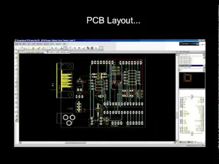
More Than Layouts: A Platform for Innovation and Precision
Today’s PCB design environments are no longer isolated schematic tools—they are sophisticated, integrated platforms that support 3D modeling, thermal analysis, signal integrity simulation, and design rule checks in a single workflow. Whether engineers are designing a flexible board for a smartwatch or a multi-layer board for automotive systems, PCB design software ensures that electrical, mechanical, and manufacturing constraints are all considered from the start.
This integration minimizes costly errors, accelerates prototyping, and helps teams deliver more reliable products to market—faster than ever before.
Electronics Are Shrinking—Software Must Scale Up
As electronics grow more compact and complex, PCB design has become exponentially more challenging. Designers now navigate tighter component spacing, higher-speed signals, and electromagnetic interference risks—all while trying to optimize power and cost.
PCB Design Software is rising to meet these challenges with features like automated routing, real-time collaboration tools, and AI-assisted layout suggestions. These capabilities empower engineers to make smarter decisions earlier in the design process, reducing the need for rework and redesign.
From Siloed Teams to Synchronized Engineering
In the past, electrical and mechanical design teams often worked in isolation, leading to disconnects between PCB layouts and enclosure designs. Today’s software breaks down those barriers. With seamless integration into mechanical CAD systems, version control platforms, and cloud-based project management tools, PCB Design Software is creating a unified engineering environment.
Collaboration is no longer a hurdle—it’s a built-in feature. Teams can co-design in real time, share libraries, and validate layouts against 3D constraints, ensuring that what’s designed digitally can be built flawlessly in the physical world.
Exhaustive Market Report: A Complete Study
https://www.futuremarketinsights.com/reports/pcb-design-software-market
Driving Compliance, Manufacturability, and Sustainability
Modern PCB design isn’t just about performance—it’s also about compliance and manufacturability. Whether it’s adhering to IPC standards, complying with regional environmental directives, or optimizing for automated assembly, design software plays a critical role.
Some platforms now offer sustainability insights, suggesting alternative materials or layouts that reduce waste and improve recyclability. This shift—from pure function to responsible innovation—is reshaping how companies approach hardware development.
The Digital Thread in Hardware’s Future
As digital twins, predictive simulations, and AI become integral to hardware development, PCB Design Software is positioned as the digital thread that connects concept to creation. It’s the tool that ensures every sensor, chip, and trace functions not only in theory, but in reality.
From startups prototyping new IoT devices to aerospace giants engineering mission-critical systems, PCB Design Software is silently enabling breakthroughs—layer by layer, trace by trace.
In a future defined by speed, complexity, and connectivity, these design platforms are no longer just tools—they are catalysts for the next generation of electronic intelligence.