The Extreme Ultraviolet Lithography (EUV) market is poised for robust growth in the coming decade, with the global valuation expected to rise from USD 12.3 billion in 2025 to USD 28.5 billion by 2035, reflecting a solid compound annual growth rate (CAGR) of 9.2%. This growth is primarily fueled by the semiconductor industry’s increasing demand for advanced lithography techniques capable of producing high-density, energy-efficient, and high-performance integrated circuits. As global demand for cutting-edge chips used in smartphones, AI, automotive electronics, and data centers continues to rise, EUV technology has emerged as a critical enabler of continued miniaturization, cost-efficiency, and improved yields.
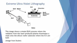
Major semiconductor manufacturers are heavily investing in EUV technology to meet the demands of next-generation chip architectures. With traditional photolithography reaching its physical and economic limits, EUV is being embraced for its ability to etch circuit patterns at wavelengths as short as 13.5 nanometers, enabling fabrication at 5nm, 3nm, and even more advanced nodes. Research and development efforts are also being accelerated to improve EUV throughput, enhance source power, and reduce system downtime. These advances are instrumental in achieving higher production efficiencies and enabling commercial viability for mass-market chip production. The technology is particularly vital for producing logic and memory chips used in smartphones, high-performance computing, autonomous vehicles, and Internet of Things (IoT) devices.
Propel Your Success: Secure Your Sample of Our Insightful Report Now!
https://www.futuremarketinsights.com/reports/sample/rep-gb-5871
Key Takeaways from the EUV Lithography Market
The Extreme Ultraviolet Lithography market is expected to grow at a CAGR of 9.2% between 2025 and 2035, reaching USD 28.5 billion by the end of the forecast period. This growth is largely driven by increased capital expenditures from leading chip manufacturers and foundries such as TSMC, Samsung, and Intel, who are relying on EUV systems to push forward their sub-5nm manufacturing capabilities. The migration toward smaller nodes is imperative for delivering faster, more power-efficient chips for emerging digital applications. Furthermore, the integration of EUV technology into back-end-of-line (BEOL) processes is gaining traction, presenting additional revenue opportunities for equipment vendors.
The Asia-Pacific region is expected to dominate the market throughout the forecast period, supported by strong investments from leading chipmakers in Taiwan, South Korea, China, and Japan. North America and Europe also play a critical role, with significant contributions from key industry players and government-backed initiatives to promote advanced semiconductor manufacturing. In addition to commercial incentives, geopolitical factors are pushing countries to establish resilient domestic semiconductor ecosystems, leading to greater adoption of EUV technology across regions.
Emerging Trends in the Global Market
Among the most notable trends in the EUV market is the push toward High-NA (High Numerical Aperture) EUV systems, which offer enhanced resolution and depth of focus, enabling even finer chip patterning and greater design flexibility. Companies are also focused on developing advanced resist materials and pellicles that can withstand the intense EUV radiation while ensuring defect-free pattern transfer. The shift from single-patterning to multi-patterning EUV lithography is another growing trend, allowing chipmakers to extend EUV usage to more layers in the semiconductor manufacturing process.
The rising popularity of 3D chip stacking and heterogeneous integration is also driving the adoption of EUV, as it allows for precise layer alignment and scaling in complex chip structures. Additionally, there is a growing emphasis on automation, predictive maintenance, and AI-based diagnostics in EUV tools to reduce operational downtime and enhance system reliability. Sustainability is also gaining importance, prompting efforts to reduce energy consumption and improve source efficiency in EUV systems, making the technology more environmentally friendly and economically scalable.
Significant Developments in the Global Sector: Trends and Opportunities
The global race for semiconductor independence has prompted several governments to incentivize domestic production, opening up new opportunities for EUV system vendors. The U.S. CHIPS Act and the European Chips Act, for instance, have earmarked billions of dollars in funding to bolster semiconductor R&D and manufacturing infrastructure, including EUV lithography. In response, companies like Intel and GlobalFoundries have announced major fab expansion plans that include EUV tool installations.
Furthermore, strategic collaborations between equipment manufacturers and chipmakers are strengthening. Companies are working together to co-develop next-generation EUV solutions, including higher wattage light sources and advanced metrology systems to improve yield control. There is also a growing opportunity for specialized service providers offering maintenance, calibration, and EUV mask handling solutions, as the ecosystem around EUV matures and expands.
Recent Developments in the Market
ASML, the undisputed leader in EUV lithography systems, continues to lead the market with the rollout of its Twinscan NXE and next-generation High-NA platforms. In 2024, the company began shipping its High-NA EUV machines to early-access customers such as Intel, signaling a major shift toward sub-2nm node development. TSMC and Samsung have also expanded their EUV production lines and are exploring further integration of EUV into DRAM and NAND flash memory processes. Additionally, semiconductor material suppliers are ramping up production of EUV-specific photoresists and pellicles to meet rising demand.
Collaborations have intensified across the supply chain. For example, Tokyo Electron, Nikon, and other equipment vendors are developing complementary tools to support EUV mask inspection and etching. Governments are also offering grants and subsidies to foster domestic innovation in EUV tool manufacturing, particularly in regions like South Korea and Japan, where local firms aim to reduce dependency on foreign suppliers.
Comprehensive Industry Report: A Full Market Analysis
https://www.futuremarketinsights.com/reports/extreme-ultraviolet-lithography-market
Competition Outlook
The EUV lithography market is characterized by limited competition due to the high entry barriers and the complexity of the technology. ASML Holding NV holds a near-monopoly in EUV lithography systems, supplying all major semiconductor foundries globally. However, competition is gradually emerging in related areas such as EUV mask blanks, pellicles, photoresists, and inspection tools, where companies like Carl Zeiss, KLA Corporation, and Tokyo Electron are key players.
Key Players
Leading players in the market include ASML Holding NV, Tokyo Electron Limited, Canon Inc., Nikon Corporation, Carl Zeiss AG, KLA Corporation, Lam Research Corporation, Applied Materials Inc., Toppan Photomasks, and JSR Corporation. These companies are heavily involved in either EUV system production or supplying critical subsystems, including optics, resists, and inspection equipment.
Key segmentations
Key segmentations in the EUV market include by equipment type (light sources, mirrors, mask systems, and others), by end-user (foundries, integrated device manufacturers, and outsourced semiconductor assembly and test providers), and by application (logic, memory, and others). Regionally, the market is divided into North America, Europe, Asia-Pacific, Latin America, and the Middle East & Africa, with Asia-Pacific maintaining the largest share due to the dominance of key semiconductor hubs.
About Future Market Insights (FMI)
Future Market Insights, Inc. (ESOMAR certified, recipient of the Stevie Award, and a member of the Greater New York Chamber of Commerce) offers profound insights into the driving factors that are boosting demand in the market. FMI stands as the leading global provider of market intelligence, advisory services, consulting, and events for the Packaging, Food and Beverage, Consumer Technology, Healthcare, Industrial, and Chemicals markets. With a vast team of 400 analysts worldwide, FMI provides global, regional, and local expertise on diverse domains and industry trends across more than 110 countries.
Contact Us:
Future Market Insights Inc.
Christiana Corporate, 200 Continental Drive,
Suite 401, Newark, Delaware – 19713, USA
T: +1-845-579-5705
For Sales Enquiries: sales@futuremarketinsights.com
Website: https://www.futuremarketinsights.com
LinkedIn| Twitter| Blogs | YouTube